Ever feel like the race for smaller and smaller computer chips is becoming an expensive game of "who has the biggest wallet"? 💸 Well, Huawei is trying to flip the script on how we build the brains of our devices.
Huawei's rotating chairman, Xu Zhijun, recently dropped some bombshell insights into a new design methodology called "He's Law" (also known as the Tau Scaling Law or τ-law). The big idea? You don't actually need the most expensive, tiny fabrication nodes to get cutting-edge performance. Instead, you can use mature 7-nanometer (7nm) tech and make it perform like a beast through smarter design. 💻✨
Wait, isn't Moore's Law the gold standard?
For decades, Moore's Law told us that transistor density doubles every two years—basically, everything just gets smaller. Xu clarifies that He's Law isn't here to replace Moore, but to provide a practical alternative. Instead of just shrinking transistors, Huawei is focusing on reducing the "time constant" (τ) across the entire system—from the device and circuit levels up to the chip itself.
The Secret Sauce: Logic Folding 📄
The most mind-blowing part of this technique is something called "logic folding." To make it easy to understand, Xu used a simple analogy:
"Folding means folding a single sheet of paper; stacking means putting two separate sheets on top of each other."
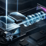
While traditional 3D stacking just piles chips on top of one another, logic folding designs multiple dies as a single integrated unit from the start. This allows for way better optimization and, more importantly, dramatically lowers the cost of production. Why spend a fortune chasing the latest node when you can fold your way to high performance? 🤯
What's next for your gadgets?
This isn't just theoretical. Huawei's HiSilicon unit is set to show off this tech commercially later this year with the Kirin 2026 chip—the first mobile processor to use logic folding. If things keep going according to plan, Huawei expects this design to reach the equivalent of 1.4nm-class transistor density by 2031. 🌟
By focusing on efficiency and smart architecture over raw size, Huawei is paving a new path for the semiconductor world, proving that sometimes, thinking differently is better than just thinking smaller. 🌍💬
Reference(s):
How will Huawei build cutting-edge chips with cheaper 7nm tech?
cgtn.com